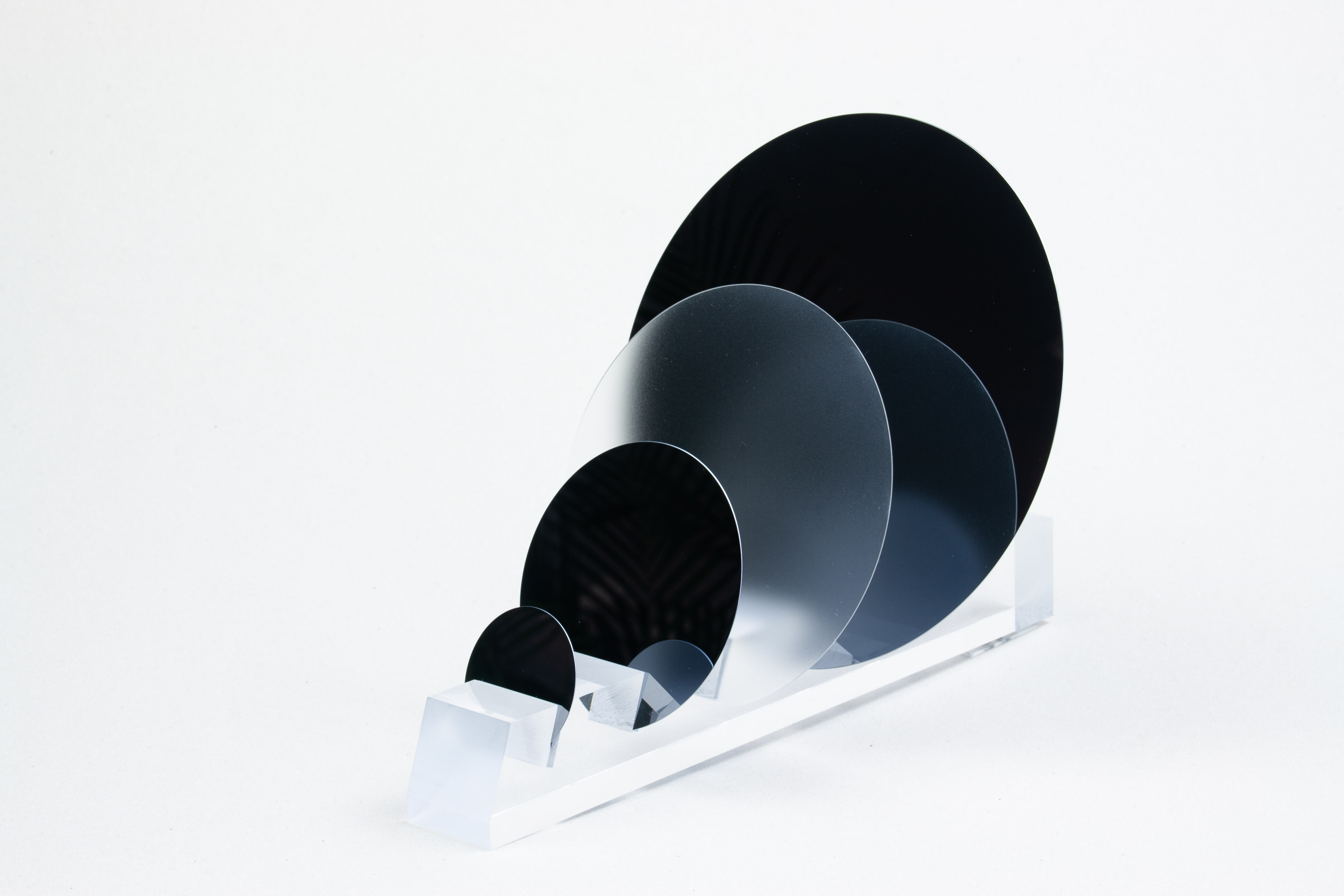
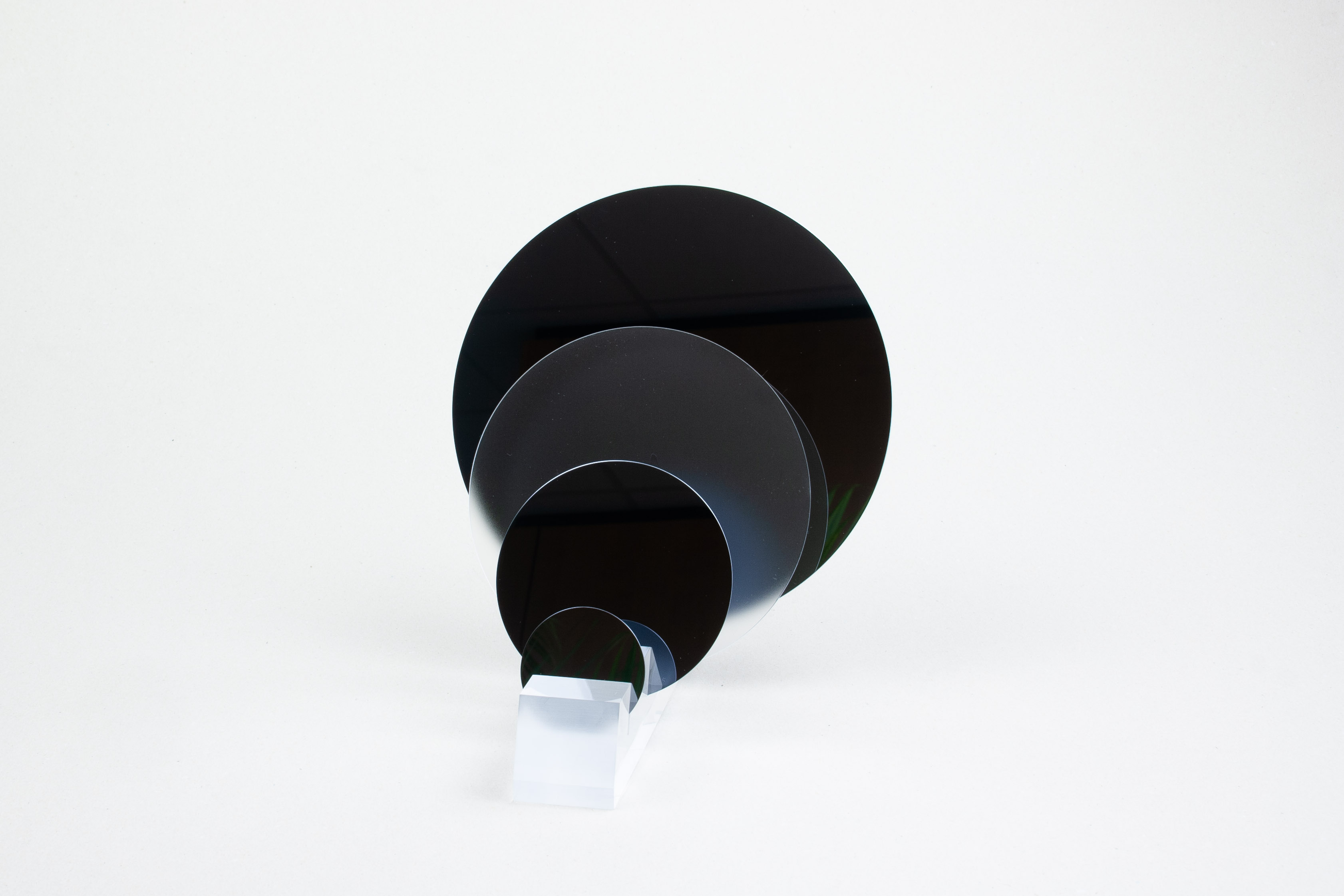
PRODUCTION OF SILICON WAFERS
From ingot to cylinder
The Si single crystals obtained from the CZ or FZ process are sawn into shorter cylinders and milled to the desired diameter.
Flats
To clearly mark the crystal orientation of the later wafers, so-called "flats" are ground into the cylinders (Fig. below). From a diameter of 8 inches, wafers are marked with a "notch" regardless of the doping . The following two processes are mainly used to cut wafer blanks from the finished milled cylinders.
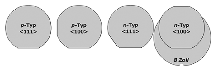
The usual ("SEMI standard") arrangement of the flats or the notch of wafers depending on their crystal orientation and doping.
Inside hole saw
Here, the wafer is sawn from the cylinder with a round saw blade , which is set with diamonds on the inside of the circular recess (diagram below). The surfaces of the wafers sawn in this way are therefore already relatively flat, so that the further grinding of the wafers takes comparatively little time. However, only one wafer can be sawn at a time per saw blade, so that the throughput of this process is low and the costs are correspondingly high .
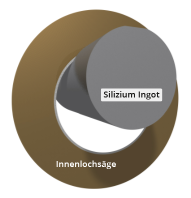
Diagram of an internal hole saw with the centrally mounted silicon ingot.
Wire saw
For this reason, wire sawing is currently predominantly used. Here, a very thin (diameter approx. 100 - 200 μm) stainless steel wire simultaneously saws many wafers out of the Si cylinder via guide rollers on which hundreds of equidistant grooves guide the wire and thus define the thickness of the wafers (see diagram below). Several Si cylinders can also be separated into wafers at the same time. Abrasion during sawing is ensured either by equipping the wire with diamond chips or by adding an abrasive with abrasive particles of diamond chips or silicon carbide. The wire is guided along the Si cylinder only once per sawing process, which means that the total length of the wire can be 100 km . The surface of the sawn wafers is less even than those cut by internal hole saws, so that more reworking is required for further smoothing.
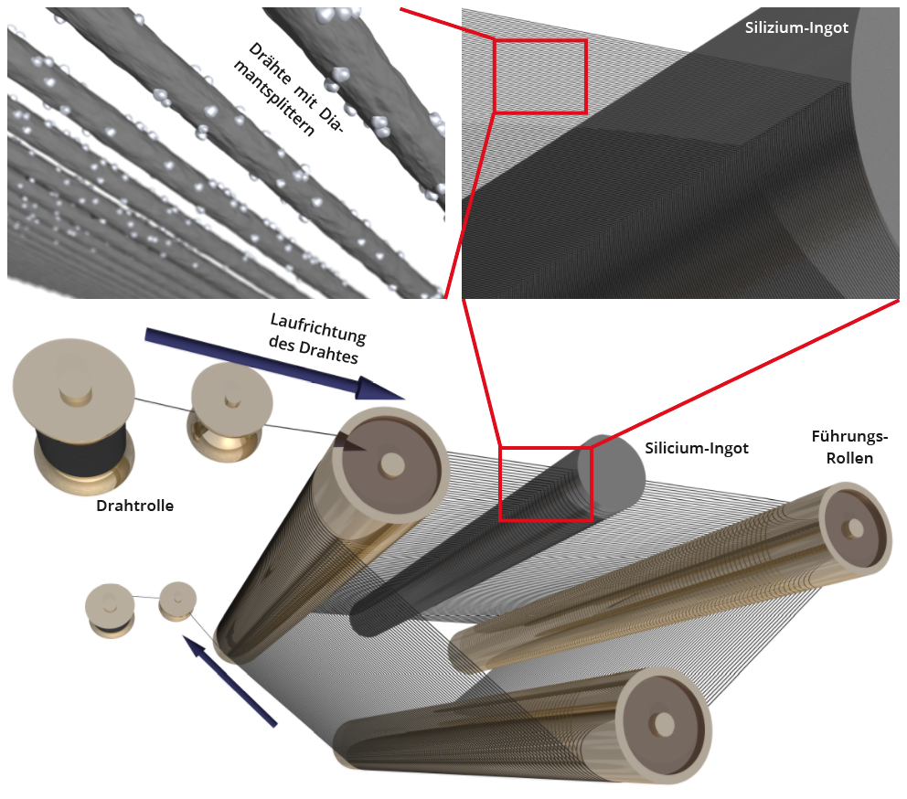
Schematic representation of the wire sawing process. The two sections above show the proportions between Si ingot, wire spacing and wire diameter approximately to scale.
Grinding
After sawing, the wafers are ground on both sides to smooth the grooves created on the surface during wire sawing, and to thin the wafers to the desired thickness. Here several wafers are processed simultaneously between counter-rotating pads by an abrasive containing, for example, Al2O3or SiC particles of a defined size distribution.
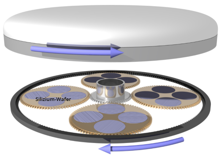
Schematic of a grinding machine (in principle also a polishing machine) for wafers. The counter-rotating and superimposed rotation ensures uniform removal without favouring a particular direction .
Etching
As the crystal structure of the Si surface was partially destroyed during sawing and grinding, wet chemical etching is carried out on both sides in e.g. KOH or HF/HNO3 mixtures down to the undisturbed Si crystal structure.
Polishing
To smooth the wafers on one or both sides to an atomic scale, they must be polished. For this purpose, the wafer is pressed onto the polishing disc with the polishing cloth on the carrier with defined pressure. The polishing agent contains several 10 to 100 nm particles of e.g. Al2O3, SiO2 or CeO2, which mechanically and chemically remove and smooth the Si surface.
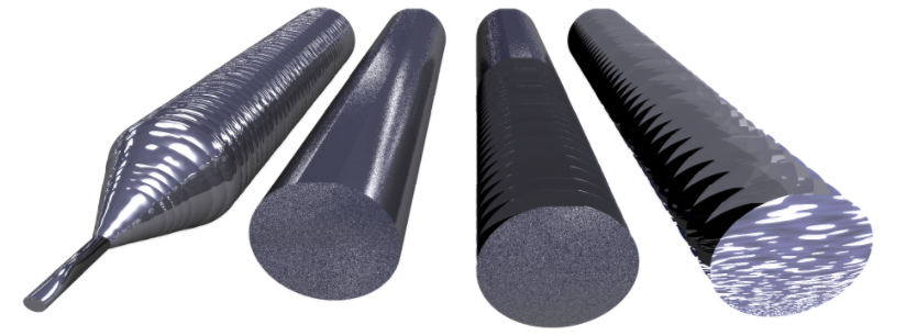
Milling, sawing, etching and polishing (from left to right) are the work steps from ingot to finished wafer.
Cleaning
Finally, the wafers are cleaned with high-purity chemicals to remove the polishing agents without leaving any residue and to ensure compliance with the required particle specification.
Further Information:
> Application areas and compatibilities
> Image Reversal Resist Processing


