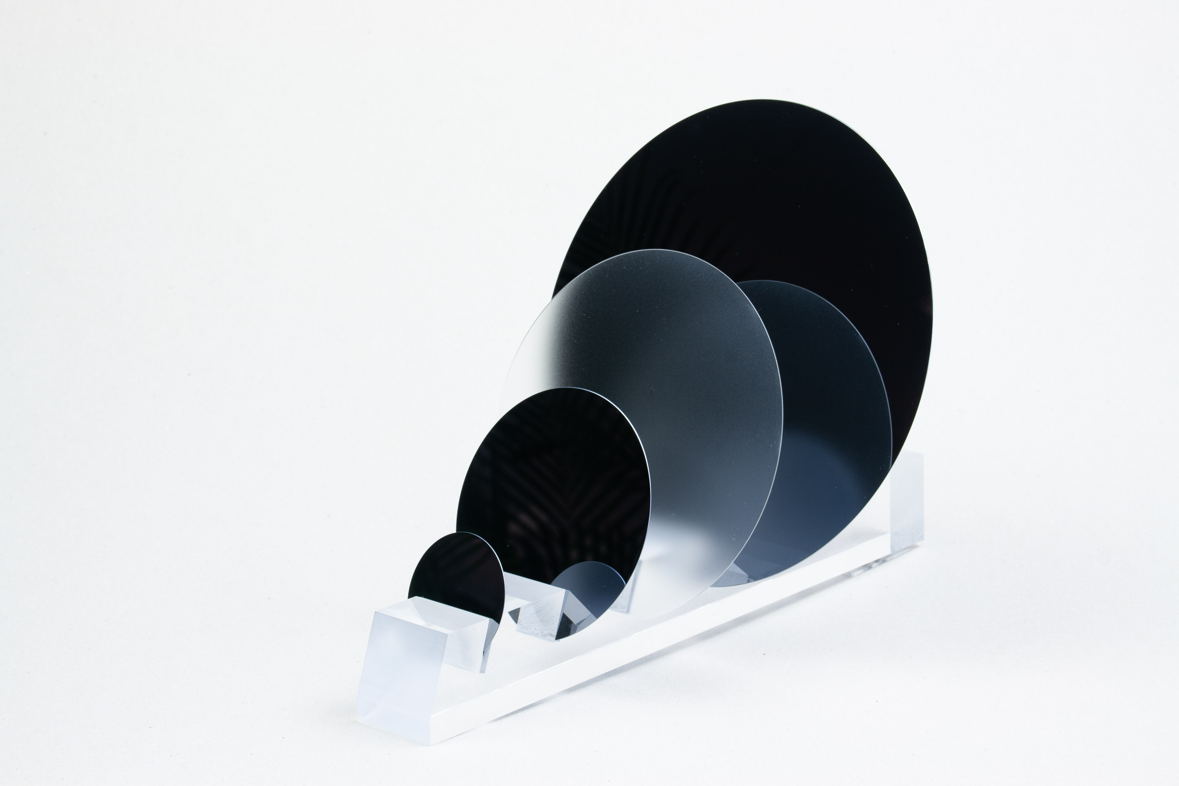
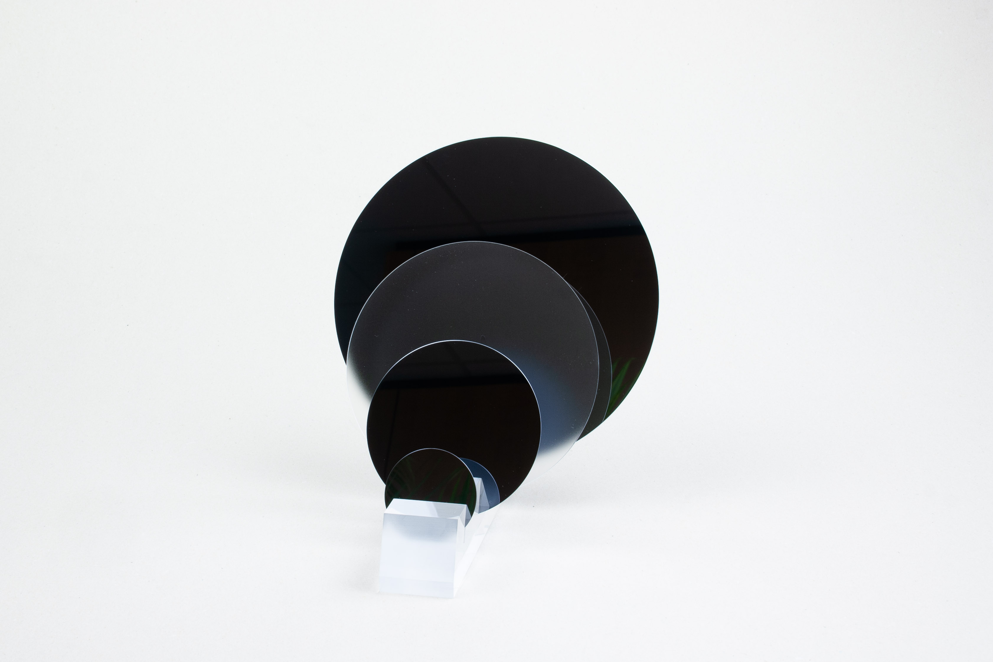
SPECIFICATIONS OF WAFERS
Diameter or edge length
The diameters of silicon wafers are specified either in inches or mm
. Although one inch corresponds to 25.4 mm, the
diameters of wafers specified in inches usually correspond to multiples of 25.0 mm
(e.g. 4 inches=100 mm), which should be clarified in advance with the supplier
.
The tolerance of the diameter is usually +/- 0.5
mm. We also offer wafers cut into rectangular pieces. The
generally realisable range of edge lengths for silicon
wafer pieces is from 5 x 5 mm2 to 100 x 120 mm2that of glass, fused silica and quartz wafer pieces from 2 x 2 mm2 to 300 x 300 mm2. The costs are defined by the starting material and the desired number of pieces.
Orientation
The orientation of a wafer (e.g. <100>, <110> or <111>) characterises the crystal plane parallel to which the wafer is sawn. For certain applications, a defined tilt to the main crystal plane may be desirable, but usually attempts are made to orientate the wafer surface as precisely as possible to the main crystal plane; the corresponding tolerances are usually +/- 0.5°.
Surface
Both sides of Si wafers are always at least lapped and
etched. Polishing is carried out either on one side (polished on one side, SSP
=Single-Side Polished) or both sides (polished on both sides, DSP=
Double-Side Polished).
The roughness of the polished side(s)
is approx. 1 nm (0.5 nm is technically feasible), that of the unpolished
side in the range of a few μm.
Doping and electrical resistance
The dopants introduced during crystal growth increase the
electrical conductivity of silicon by many orders of magnitude above the
value of undoped silicon via
free electrons (in the case of phosphorus or arsenic) or holes (boron). Below a dopant concentration
of approx. c=1016 cm-3 the resistance R decreases
reciprocally with c, above which the mobility of the
charge carriers decreases increasingly due to the high
concentration of impurities, which flattens the dependence R(c) (Fig. below).
Since the
dopant concentration in the Si crystal varies both axially and radially
, only a certain tolerance range can be specified for the electrical resistance of the
wafers produced from it, which
typically lies within an order of magnitude (e.g. 1 - 10 Ohm
cm), but can also only span a factor
of approx. two due to more defined manufacturing processes and, if necessary, subsequent sorting of the wafers in a batch
.
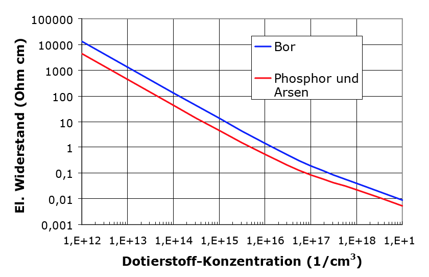
The dependence of the electrical resistance on the dopant concentration (boron and phosphorus or arsenic) in crystalline silicon. Since at very high dopant concentrations these act as impurities which reduce the mobility of the charge carriers , the specific resistance decreases from a dopant concentration of approx. 1016 increasingly slower.
Wafer thickness
For reasons of mechanical
stability during production and further processing, the usual thickness of Si wafers depends on their
diameter and is approx. 280 μm (2 inches), 380 μm (3 inches), 525 μm
(4 inches), 675 μm (6 inches) and 725 μm (8 inches).
In standard
manufacturing processes, the wafer thickness is limited upwards to approx. 2 mm
as the polishing machines cannot accommodate thicker wafers.
Many manufacturers limit the wafer thickness downwards to approx. 200 μm
due to the risk of breakage during grinding
and polishing.
The thickness tolerance corresponds to the variation of the thickness measured in the
wafer centre over a batch.
This value is usually specified as +/-
25 μm, largely independent of the wafer diameter; the measured values are often around +/- 15 μm.
However, this
distribution says nothing about how much a wafer deviates from the
ideal cylinder shape. This is characterised by the TTV, Bow and Warp values described in the following
with the aid of the
surfaces and planes defined in the figure below.
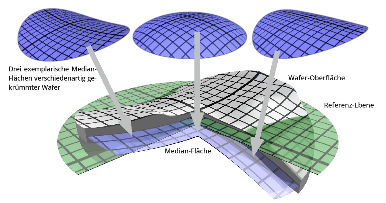
In addition to the thickness inhomogeneity of a wafer (grey shape), a wafer can be curved differently in itself, which can be represented by so-called median areas (blue) that do not take the thickness inhomogeneity into account. The deviation of the median area of a wafer from the planar reference plane (green) defines the parameters Bow and Warp.
TTV
The Total Thickness Variation characterises the maximum difference d1 - d2 (Fig. below, top illustration) between the thickest and thinnest point of a wafer. Up to a diameter of 4 inches, wafers are usually specified to TTV < 10 μm (although TTV < 5 μm can also be realised without great technical effort), with larger diameters the achievable values for TTV also increase.
Bow
The Bow bending is defined by the maximum deviation of the median surface of the wafer from a reference plane determined via d3 + d4 (Fig. below, centre illustration). Up to a diameter of 4 inches, wafers are usually specified to Bow < 40 μm, with larger diameters, the achievable values for Bow also increase.
Warp
The value d5 + d6 (Fig. below, bottom diagram) is the deviation of the median area of a wafer from a reference plane where the bending over the entire wafer area has already been corrected. Up to a diameter of 4 inches , wafers are usually specified for warp < 40 μm; with larger diameters, the achievable values for warp also increase.
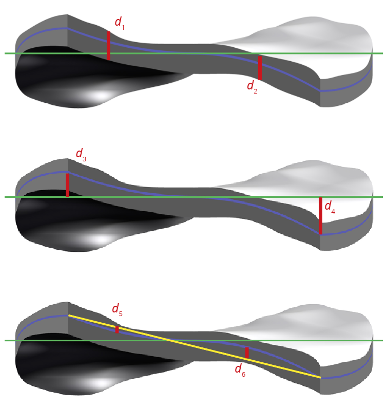
Schematic representation of wafers with strongly exaggerated thickness inhomogeneity and curvature to visualise the parameters d1... d6 from which the parameters TTV, Bow and Warp are derived.
Microroughness
Regardless of the thickness inhomogeneity, which is expressed in the size TTV on a cm scale via
the wafer, there is a roughness on
a much smaller μm and nm scale, which has its origin in the
polishing step during wafer production.
The
root mean square (RMS) of the surface characterises how smooth the wafer is as a
standard deviation of the wafer surface from the mean value (already
adjusted for TTV, bow and
warp). For the polished
wafer side, RMS is usually specified at < 1 nm; technically feasible
are also < 0.5 nm, which is already on an atomic scale.
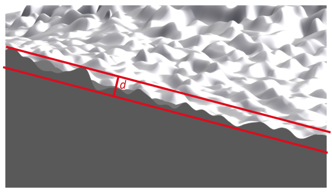
The polishing process during wafer production creates a very smooth surface with a roughness of a few nm or less.
Laser marking
On request, our wafers can be laser-marked . This is usually a marking followed by a serial number. In principle, the laser marking can be applied to the polished front side or the back side, although marking of the polished side is only recommended to a limited extent: laser marking creates burrs at the edges of the marking, so laser marking should take place before the polishing step of the wafer. During polishing, however, the wafers thin out and the legibility of the laser marking decreases with the removal during polishing. For larger batches (e.g. > 200 wafers), laser marking can usually be carried out for well under € 1.00 / wafer. Subsequent laser marking of wafers that we already have in stock is somewhat more expensive.
Further Information:
> Application areas and compatibilities
> Image Reversal Resist Processing
Filter products


