COATED WAFERS
Thermal oxidation
Areas of application
The electrical (1014 - 1016 Ohm cm, dielectric strength106 -107
V/cm, barrier for electrons and holes from monocrystalline Si > 3
eV), mechanical (melting point approx. 1700 °C) and optical (transparent
in the visible as well as near and mid IR and UV spectral range)
properties of SiO2 make it a suitable material
for use as a dielectric layer in transistors,
capacitors (DRAM) or flash memories, as a hard mask for diffusion
and implantation processes or as a wet or dry chemical etchant. wet or dry chemical etching,
generally as electrical insulation between components or
anti-reflective layer on solar cells, for example.
The required layer thicknesses
range from a few nm (gate oxide in state-of-the-art
CMOS transistors) to a few µm for electrical insulation between
components.
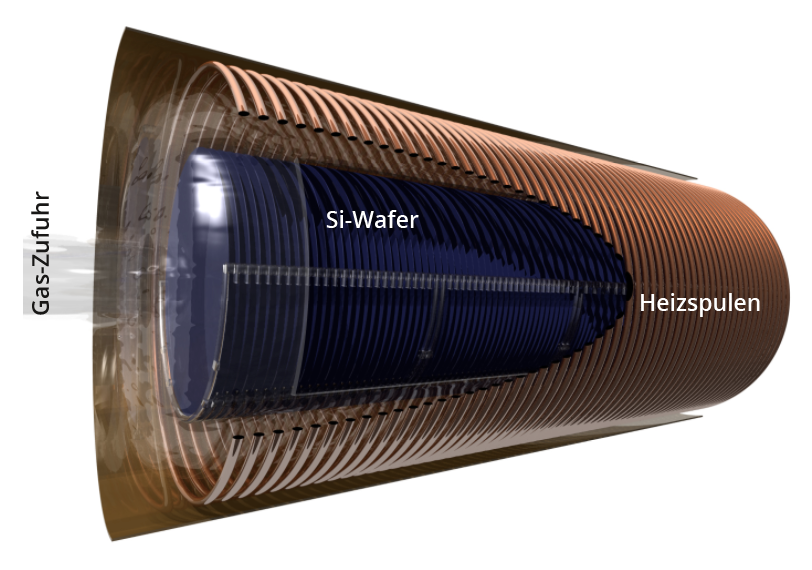
Schematic design of a furnace for the thermal oxidation of silicon wafers.
Technical realisation
Native (grown at room temperature in air, a few nm thick) and thermal (growth at 800 ... 1200°C) oxide are - in contrast to crystalline quartz - amorphous phases of SiO2 without long-range ordering of the atomic lattice. As the Si of the SiO2 in the native and thermal oxide comes from the substrate, this is consumed while the overall thickness increases due to the oxide: In the process, 100 nm of SiO2 require approx. 46 nm of Si. The thickness of the wafer increases by approx. 54 nm.
A distinction is made between dry o xide (Si + O2 → SiO2) and - with H2Oas the process gas - wet o xide (Si + 2 H2O→ SiO2 + 2 H2). With otherwise identical process parameters, the latter has a slightly higher porosity due to the higher growth rate and therefore also a higher etching rate in HF.
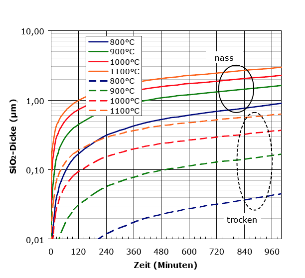
The layer thicknesses achieved with "wet" (solid lines) and "dry" (dashed) SiO2 as a function of the growth time and temperature.
Growth rate and achievable oxide layer thicknesses
At the beginning of SiO2 growth, the chemical reaction rate limits the growth rate; the layer thickness grows linearly with time. As the oxide thickness increases, the diffusion of oxygen through the already grown oxide to the Si/SiO2 interface slows down the growth rate; the SiO2 thickness now only grows with the square root of time. In addition to the process gases (O2/H2O) and their partial pressure as well as the substrate temperature (thermally activated diffusion and reaction rates), the growth rate of the oxide also depends on the crystallisation direction of the Si substrate relative to the growth direction, mechanical stresses (if the silicon has already been microstructured) and doping (faster oxide growth, e.g. from phosphorus-doped silicon).
PECVD coating with SiO2
Mechanism
As an alternative to the thermal oxidation of silicon, SiO2 layers can also be deposited on silicon via the gas phase (PECVD=Plasma Enhanced Chemical Vapour Deposition) via SiH4 + 2 N2O→ SiO2 + 2 N2.
Advantages compared to thermal SiO2
As the layer thickness increases linearly with time during PECVD deposition, very thick layers of several µm can be grown significantly faster than via thermal oxidation. If only a few wafers are to be coated, PECVD deposition is more favourable than thermal oxidation, in which larger quantities (e.g. 100 wafers) can be processed at the same time. Thermal SiO2 always contains the impurities (dopants) of the silicon substrate, whereas the composition of SiO2 layers grown using PECVD is independent of the substrate.
Disadvantages compared to thermal SiO2
PECVD SiO2 grows more amorphously than thermal oxide, which has an effect on the electrical and chemical properties:
Compared to thermal SiO2, PECVD SiO2
has a lower electrical breakdown strength, which is why the gate oxides, some of which are
a few nm thick, are preferably produced thermally. In addition,
the etch rate of PECVD SiO2 is significantly higher than that of thermal oxide, which is why it is not so well suited as an etching mask for anisotropic Si etching, for example.
Deposition of silicon nitride
Use of silicon nitride
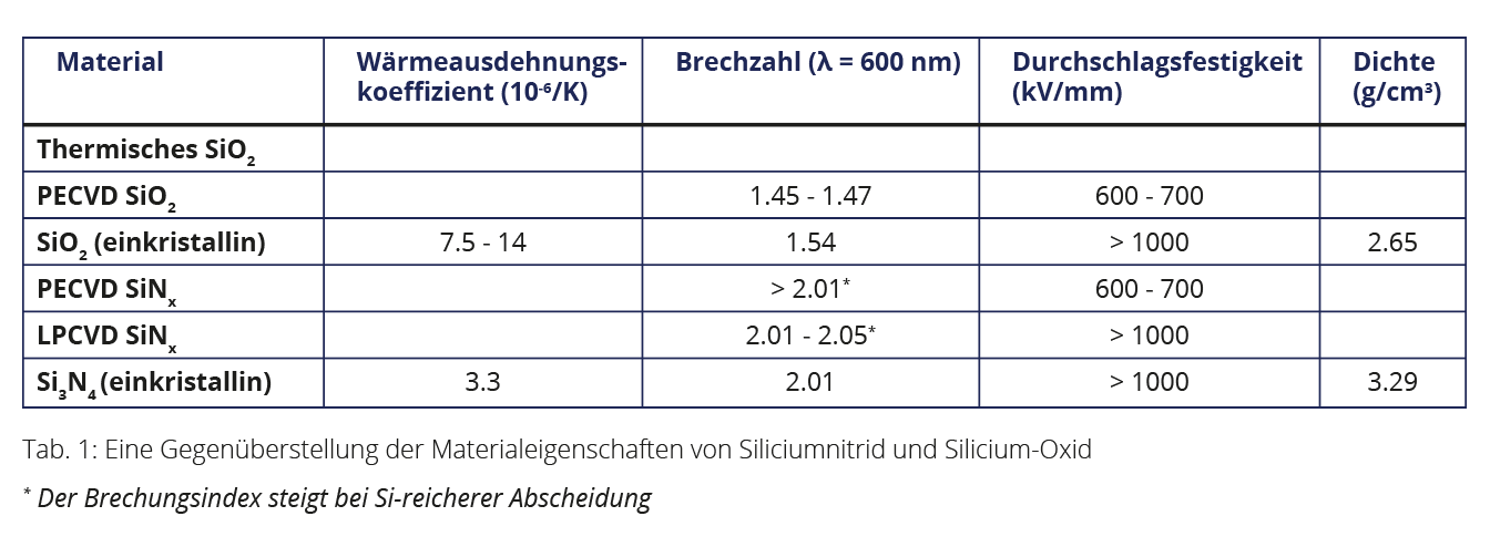
While stoichiometric silicon nitride (Si3N4) is used in toolmaking due to its high hardness and thermal stability in extremely stressed roller bearings or cutting tools , for example, it is primarily the chemical, electrical and optical properties that make this material interesting for various areas of application in semiconductor technology. In integrated circuits, amorphous silicon nitride is used as a passivation or insulation layer, as a masking and etch-stop material in lithographic processes due to its high stability in alkaline or hydrofluoric acid-containing media, as a masking material for oxidation processes due to its low diffusion constant for oxygen, and as an anti-reflective coating in photovoltaics due to its adjustable refractive index.
PECVD silicon nitride
The amorphous silicon nitride (SiNx) deposited from SiH4 and NH3 using PECVD (Plasma Enhanced Chemical Vapour Deposition) typically contains 5 - 20 atomic % hydrogen (therefore sometimes called SiNx:H), depending on the deposition temperature and gas composition, which saturates the open bonds and thus chemically and physically stabilises the lattice. SiNx can be etched, e.g. via photoresist masks, either using hydrofluoric acid or selectively to SiO2 with hot concentrated phosphoric acid. The etching rate of SiNx in hydrofluoric acid depends crucially on the deposition temperature and the refractive index. A hydrogen-rich silicon nitride layer, deposited at 100°C with a refractive index of n=1.9 has an etch rate of several 100 nm/min in buffered hydrofluoric acid (12.5 % HF). In contrast, a layer deposited at 400°C with a refractive index of n=2 shows an etching rate of only approx. 10 nm/min.
LPCVD silicon nitride
LPCVD (Low Pressure Chemical Vapour Deposition) silicon nitride is deposited at significantly higher temperatures
around 700 - 850°C using the reaction equation 3 SiH2Cl2 + 4 NH3 → S3iN4 + 6 HCl + 6 H2
compared to PECVD deposition. As a result, the layer grows significantly
less hydrogen and more stoichiometrically than PECVD nitride and exhibits very
good electrical properties, very good edge coverage,
high thermal stability and a low etch rate in hydrofluoric acid.
The
deposition takes place via the sub-steps 1) gas supply of the reactants,
2) physical bonding of the molecules on the surface, 3) chemical
bonding on the surface and 4) desorption and removal of the
by-products. The growth rate is limited almost exclusively by
the chemical reaction on the growing layer and not by the supply
and consumption of the starting materials; a significant depletion
of the reactants does not take place due to the lower growth rate compared to PECVD deposition
. Therefore,
many (e.g. 25 or 50) wafers can be processed simultaneously in the gas flow of a reactor with very high
layer thickness homogeneity across the wafer surface, i.e. also from wafer
to wafer of a batch.
The deposition can be controlled in such a way
that either mechanically unstressed (low stress),
or almost stoichiometric (Si3N4) silicon nitride is produced.
Further Information:
> Application areas and compatibilities
> Image Reversal Resist Processing
Filter products


